Wednesday, July 14, 2010

Moore Machine

The following state diagram (Fig. 1) describes a finite state machine with one input X and one output Z. The FSM asserts its output Z when it recognizes the following input bit sequence: "1011". The machine will keep checking for the proper bit sequence and does not reset to the initial state after it has recognized the string. As an example the input string X= "..1011011..." will cause the output to go high twice: Z = "..0001001.." . The output will asserts only when it is in state S4 (after having seen the sequence 1011). The FSM is thus a Moore machine.

Figure 1: State diagram, describing the sequence detector implemented as a Moore machine. The number in italics underneath the states indicate which part of the sequence the state remembers.

This state diagram can be described in ABEL code given in Listing 1. The output is described after the STATE Si: statement.

Listing 1: ABEL source code for the Moore machine implementation of the sequence detector described in Fig. 1

    module Seqdet2
    Title 'Sequence detector implemented as Moore machine'
    Declarations
    "input and output signals

    X, CLOCK, RST PIN;
    Z PIN istype 'com';
    Q2, Q1, Q0 PIN istype 'reg';

    "State register declarations

    SREG = [Q2,Q1,Q0];
    S0 = [0,0,0];
    S1 = [0,0,1];
    S2 = [0,1,0];
    S3 = [0,1,1];
    S4 = [1,0,0];

    Equations
    "Definition of the state machine clock signal

    [Q2,Q1,Q0].AR = RST;
    [Q2,Q1,Q0].CLK = CLOCK;

    "Define state diagram
    STATE_DIAGRAM SREG

    STATE S0: Z=0;


      IF X THEN S1 ELSE S0;
    STATE S1: Z=0;
      IF X THEN S1 ELSE S2;
    STATE S2: Z=0;
      IF X THEN S3 ELSE S0;
    STATE S3: Z=0;
      IF X THEN S4 ELSE S2;
    STATE S4: Z=1;
      IF X THEN S1 ELSE S2;
    end Seqdet2
The corresponding simulation is shown in Figure 2.


Figure 2: Simulation of the sequence detector (for "1011") described with the state diagram of Fig. 1. (Screen clip from Xilinx XACTstep(TM) Foundation software)

Mealy machine

The following state diagram (Fig. 1) describes a finite state machine with one input X and one output Z. The FSM asserts its output Z when it recognizes the following input bit sequence: "1011". The machine will keep checking for the proper bit sequence and does not reset to the initial state after it has recognized the string. As an example the input string X= "..1011011..." will cause the output to go high twice: Z = "..0001001.." . When the machine is in the state S3 the output will go high after the arrival of a "1" at the input. Thus the output is associated with the transitions as indicated on the state diagram.


Figure 1: State diagram, describing the sequence detector implemented as a Mealy machine.
The number in italics underneath the states indicate which part of the sequence the state remembers.

This state diagram can be described in ABEL code given in Listing 1. The output is described with the "With" keyword to indicate that the output will change when the input goes to one.

Listing 1: ABEL source code for the Mealy Machine implementation of the sequence detector described in Fig. 1

    module Seqdet1
    Title 'Sequence Detector 1011 with Mealy Machine'

    Declarations
    "Input and output signals

    X, CLOCK, RST PIN;
    Z PIN istype 'com';
    Q1, Q0 PIN istype 'reg';

    "State register definitions
    " and assignments of state values

    SREG = [Q1,Q0];
    S0 = [0,0];
    S1 = [0,1];
    S2 = [1,0];
    S3 = [1,1];

    Equations
    "Define the clock signal for the state machine

    [Q1,Q0].AR = RST;
    [Q1,Q0].CLK =CLOCK;

    "Define state diagram

    STATE_DIAGRAM SREG

    STATE S0: IF X THEN S1 ELSE S0;
    STATE S1: IF X THEN S1 ELSE S2;
    STATE S2: IF X THEN S3 ELSE S0;
    STATE S3: IF X THEN S1 WITH Z=1; ELSE S2;

    end Seqdet1

The ouput is specified with the "With" keyword. The corresponding simulation is shown in Figure 2.

Figure 2: Simulation of the sequence detector for "1011" described with the state diagram of Fig. 1.
(Screen clip from Xilinx XACTstep(TM) Foundation software)

Notice that the output Z asserts as soon as the input is "1" when in state S3. Comparing this output with the one obtained for a Moore machine of the same sequence detector may let a casual observer think that there is a timing problem as the output seems to asserts already after the "101" input sequence. However, when one looks at the output carefully one concludes that the waveform is correct. One has to realize that the outputs are valid at the end of the state time (just before the positive clock-edge) while the valid inputs are sampled just before the positive clock edge as indicated in Figure 3 below. The input sequence "1011" gives indeed an output sequence of "0001".

Figure 3: Output waveform of the Mealy machine (sequence detector for "1011") with valid inputs and outputs indicated.
(Screen clip from Xilinx XACTstep(TM) Foundation software)

One notices that there is a glitch in the output after the input sequence 10111010. However this occurs at a moment that the output is not valid (the output is valid just before the positive clock edge). The valid output sequence is than 000100000 as expected.

Tuesday, February 23, 2010

AMPLIFIER COUPLING

Earlier in this module it was stated that almost every electronic device contains at least one stage of amplification. Many devices contain several stages of amplification and therefore several amplifiers. Stages of amplification are added when a single stage will not provide the required amount of amplification. For example, if a single stage of amplification will provide a maximum gain of 100 and the desired gain from the device is 1000, two stages of amplification will be required. The two stages might have gains of 10 and 100, 20 and 50, or 25 and 40. (The overall gain is the product of the individual stages-10 X 100 = 20 X 50 = 25 X 40 = 1000.)

Figure 1-8 shows the effect of adding stages of amplification. As stages of amplification are added, the signal increases and the final output (from the speaker) is increased.

Figure 1-8. - Adding stages of amplification.

Whether an amplifier is one of a series in a device or a single stage connected between two other devices (top view, figure 1-8), there must be some way for the signal to enter and leave the amplifier. The process of transferring energy between circuits is known as COUPLING. There are various ways of coupling signals into and out of amplifier circuits. The following is a description of some of the more common methods of amplifier coupling.

Direct Coupling

The method of coupling that uses the least number of circuit elements and that is, perhaps, the easiest to understand is direct coupling. In direct coupling the output of one stage is connected directly to the input of the following stage. Figure 1-9 shows two direct-coupled transistor amplifiers.

Figure 1-9. - Direct-coupled transistor amplifiers.

Notice that the output (collector) of Q1 is connected directly to the input (base) of Q2. The network of R4, R5, and R6 is a voltage divider used to provide the bias and operating voltages for Q1 and Q2. The entire circuit provides two stages of amplification.

Direct coupling provides a good Frequency response since no frequency-sensitive components (inductors and capacitors) are used. The Frequency response of a circuit using direct coupling is affected only by the amplifying device itself.

Direct coupling has several disadvantages, however. The major problem is the power supply requirements for direct-coupled amplifiers. Each succeeding stage requires a higher voltage. The load and voltage divider resistors use a large amount of power and the biasing can become very complicated. In addition, it is difficult to match the impedance from stage to stage with direct coupling. (Impedance matching is covered a little later in this chapter.)

The direct-coupled amplifier is not very efficient and the losses increase as the number of stages increase. Because of the disadvantages, direct coupling is not used very often.

RC Coupling

The most commonly used coupling in amplifiers is RC coupling. An RC-coupling network is shown in figure 1-10.

Figure 1-10. - RC-coupled transistor amplifier.

The network of R1, R2, and C1 enclosed in the dashed lines of the figure is the coupling network. You may notice that the circuitry for Q1 and Q2 is incomplete. That is intentional so that you can concentrate on the coupling network.

R1 acts as a load resistor for Q1 (the first stage) and develops the output signal of that stage. Do you remember how a capacitor reacts to ac and dc? The capacitor, C1, "blocks" the dc of Q1's collector, but "passes" the ac output signal. R2 develops this passed, or coupled, signal as the input signal to Q2 (the second stage). This arrangement allows the coupling of the signal while it isolates the biasing of each stage.

This solves many of the problems associated with direct coupling.

RC coupling does have a few disadvantages. The resistors use dc power and so the amplifier has low efficiency. The capacitor tends to limit the low-Frequency response of the amplifier and the amplifying device itself limits the high-Frequency response. For audio amplifiers this is usually not a problem; techniques for overcoming these frequency limitations will be covered later in this module.

Before you move on to the next type of coupling, consider the capacitor in the RC coupling. You probably remember that capacitive reactance (XC) is determined by the following formula:

This explains why the low frequencies are limited by the capacitor. As frequency decreases, XC increases. This causes more of the signal to be "lost" in the capacitor.

The formula for XC also shows that the value of capacitance (C) should be relatively high so that capacitive reactance (XC) can be kept as low as possible. So, when a capacitor is used as a coupling element, the capacitance should be relatively high so that it will couple the entire signal well and not reduce or distort the signal.

Impedance Coupling

Impedance coupling is very similar to RC coupling. The difference is the use of an impedance device (a coil) to replace the load resistor of the first stage.

Figure 1-11 shows an impedance-coupling network between two stages of amplification. L1 is the load for Q1 and develops the output signal of the first stage. Since the d.c. resistance of a coil is low, the efficiency of the amplifier stage is increased. The amount of signal developed in the output of the stage depends on the inductive reactance of L1. Remember the formula for inductive reactance:

Figure 1-11. - Impedance-coupled transistor amplifier.

The formula shows that for inductive reactance to be large, either inductance or frequency or both must be high. Therefore, load inductors should have relatively large amounts of inductance and are most effective at high frequencies. This explains why impedance coupling is usually not used for audio amplifiers.

The rest of the coupling network (C1 and R1) functions just as their counterparts (C1 and R2) in the RC-coupling network. C1 couples the signal between stages while blocking the d.c. and R1 develops the input signal to the second stage (Q2).

Transformer Coupling

Figure 1-12 shows a transformer-coupling network between two stages of amplification. The transformer action of T1 couples the signal from the first stage to the second stage. In figure 1-12, the primary of T1 acts as the load for the first stage (Q1) and the secondary of T1 acts as the developing impedance for the second stage (Q2). No capacitor is needed because transformer action couples the signal between the primary and secondary of T1.

Figure 1-12. - Transformer-coupled transistor amplifier.

The inductors that make up the primary and secondary of the transformer have very little dc resistance, so the efficiency of the amplifiers is very high. Transformer coupling is very often used for the final output (between the final amplifier stage and the output device) because of the impedance-matching qualities of the transformer. The Frequency response of transformer-coupled amplifiers is limited by the inductive reactance of the transformer just as it was limited in impedance coupling.

Saturday, February 20, 2010

demorgan's law in boolean algebra

The most obvious way to simplify Boolean expressions is to manipulate them in the same way as normal algebraic expressions are manipulated. With regards to logic relations in digital forms, a set of rules for symbolic manipulation is needed in order to solve for the unknowns.
A set of rules formulated by the English mathematician George Boole describe certain propositions whose outcome would be either true or false. With regard to digital logic, these rules are used to describe circuits whose state can be either, 1 (true) or 0 (false). In order to fully understand this, the relation between the AND gate, OR gate and NOT gate operations should be appreciated. A number of rules can be derived from these relations as Table 1 demonstrates.
  • P1: X = 0 or X = 1
  • P2: 0 . 0 = 0
  • P3: 1 + 1 = 1
  • P4: 0 + 0 = 0
  • P5: 1 . 1 = 1
  • P6: 1 . 0 = 0 . 1 = 0
  • P7: 1 + 0 = 0 + 1 = 1
Table 1: Boolean Postulates

Laws of Boolean Algebra

Table shows the basic Boolean laws. Note that every law has two expressions, (a) and (b). This is known as duality. These are obtained by changing every AND(.) to OR(+), every OR(+) to AND(.) and all 1's to 0's and vice-versa.
It has become conventional to drop the . (AND symbol) i.e. A.B is written as AB.
T1 : Commutative Law
(a) A + B = B + A
(b) A B = B A
T2 : Associate Law
(a) (A + B) + C = A + (B + C)
(b) (A B) C = A (B C)
T3 : Distributive Law
(a) A (B + C) = A B + A C
(b) A + (B C) = (A + B) (A + C)
T4 : Identity Law
(a) A + A = A
(b) A A = A
T5 :
(a)
(b)
T6 : Redundance Law
(a) A + A B = A
(b) A (A + B) = A
T7 :
(a) 0 + A = A
(b) 0 A = 0
T8 :
(a) 1 + A = 1
(b) 1 A = A
T9 :
(a)
(b)
T10 :
(a)
(b)
T11 : De Morgan's Theorem
(a)
(b)

Table 2: Boolean Laws


Examples Examples

Prove T10 : (a)

(1) Algebraically:

(2) Using the truth table:
Truth table

Using the laws given above, complicated expressions can be simplified.

Thursday, February 18, 2010

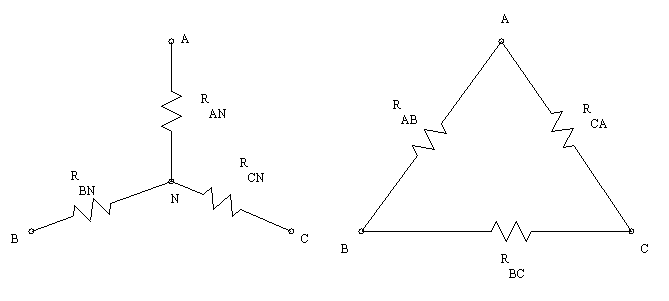
Star and Delta Transformation Formulas

Kennelly's Star-Delta Transformation

Kennelly's Delta - Star Transformation

Kirchhoff's Current Law (KCL)

Let's take a closer look at that last parallel example circuit:

Solving for all values of voltage and current in this circuit:

At this point, we know the value of each branch current and of the total current in the circuit. We know that the total current in a parallel circuit must equal the sum of the branch currents, but there's more going on in this circuit than just that. Taking a look at the currents at each wire junction point (node) in the circuit, we should be able to see something else:

At each node on the negative "rail" (wire 8-7-6-5) we have current splitting off the main flow to each successive branch resistor. At each node on the positive "rail" (wire 1-2-3-4) we have current merging together to form the main flow from each successive branch resistor. This fact should be fairly obvious if you think of the water pipe circuit analogy with every branch node acting as a "tee" fitting, the water flow splitting or merging with the main piping as it travels from the output of the water pump toward the return reservoir or sump.

If we were to take a closer look at one particular "tee" node, such as node 3, we see that the current entering the node is equal in magnitude to the current exiting the node:

From the right and from the bottom, we have two currents entering the wire connection labeled as node 3. To the left, we have a single current exiting the node equal in magnitude to the sum of the two currents entering. To refer to the plumbing analogy: so long as there are no leaks in the piping, what flow enters the fitting must also exit the fitting. This holds true for any node ("fitting"), no matter how many flows are entering or exiting. Mathematically, we can express this general relationship as such:

Mr. Kirchhoff decided to express it in a slightly different form (though mathematically equivalent), calling it Kirchhoff's Current Law (KCL):

Summarized in a phrase, Kirchhoff's Current Law reads as such:

"The algebraic sum of all currents entering and exiting a node must equal zero"

That is, if we assign a mathematical sign (polarity) to each current, denoting whether they enter (+) or exit (-) a node, we can add them together to arrive at a total of zero, guaranteed.

Taking our example node (number 3), we can determine the magnitude of the current exiting from the left by setting up a KCL equation with that current as the unknown value:

The negative (-) sign on the value of 5 milliamps tells us that the current is exiting the node, as opposed to the 2 milliamp and 3 milliamp currents, which must both positive (and therefore entering the node). Whether negative or positive denotes current entering or exiting is entirely arbitrary, so long as they are opposite signs for opposite directions and we stay consistent in our notation, KCL will work.

Together, Kirchhoff's Voltage and Current Laws are a formidable pair of tools useful in analyzing electric circuits. Their usefulness will become all the more apparent in a later chapter ("Network Analysis"), but suffice it to say that these Laws deserve to be memorized by the electronics student every bit as much as Ohm's Law.

Kirchhoff's Voltage Law (KVL)

Let's take another look at our example series circuit, this time numbering the points in the circuit for voltage reference:

If we were to connect a voltmeter between points 2 and 1, red test lead to point 2 and black test lead to point 1, the meter would register +45 volts. Typically the "+" sign is not shown, but rather implied, for positive readings in digital meter displays. However, for this lesson the polarity of the voltage reading is very important and so I will show positive numbers explicitly:

When a voltage is specified with a double subscript (the characters "2-1" in the notation "E2-1"), it means the voltage at the first point (2) as measured in reference to the second point (1). A voltage specified as "Ecd" would mean the voltage as indicated by a digital meter with the red test lead on point "c" and the black test lead on point "d": the voltage at "c" in reference to "d".

If we were to take that same voltmeter and measure the voltage drop across each resistor, stepping around the circuit in a clockwise direction with the red test lead of our meter on the point ahead and the black test lead on the point behind, we would obtain the following readings:


We should already be familiar with the general principle for series circuits stating that individual voltage drops add up to the total applied voltage, but measuring voltage drops in this manner and paying attention to the polarity (mathematical sign) of the readings reveals another facet of this principle: that the voltages measured as such all add up to zero:

This principle is known as Kirchhoff's Voltage Law (discovered in 1847 by Gustav R. Kirchhoff, a German physicist), and it can be stated as such:

"The algebraic sum of all voltages in a loop must equal zero"

By algebraic, I mean accounting for signs (polarities) as well as magnitudes. By loop, I mean any path traced from one point in a circuit around to other points in that circuit, and finally back to the initial point. In the above example the loop was formed by following points in this order: 1-2-3-4-1. It doesn't matter which point we start at or which direction we proceed in tracing the loop; the voltage sum will still equal zero. To demonstrate, we can tally up the voltages in loop 3-2-1-4-3 of the same circuit:

This may make more sense if we re-draw our example series circuit so that all components are represented in a straight line:

It's still the same series circuit, just with the components arranged in a different form. Notice the polarities of the resistor voltage drops with respect to the battery: the battery's voltage is negative on the left and positive on the right, whereas all the resistor voltage drops are oriented the other way: positive on the left and negative on the right. This is because the resistors are resisting the flow of electrons being pushed by the battery. In other words, the "push" exerted by the resistors against the flow of electrons must be in a direction opposite the source of electromotive force.

Here we see what a digital voltmeter would indicate across each component in this circuit, black lead on the left and red lead on the right, as laid out in horizontal fashion:

If we were to take that same voltmeter and read voltage across combinations of components, starting with only R1 on the left and progressing across the whole string of components, we will see how the voltages add algebraically (to zero):

The fact that series voltages add up should be no mystery, but we notice that the polarity of these voltages makes a lot of difference in how the figures add. While reading voltage across R1, R1--R2, and R1--R2--R3 (I'm using a "double-dash" symbol "--" to represent the series connection between resistors R1, R2, and R3), we see how the voltages measure successively larger (albeit negative) magnitudes, because the polarities of the individual voltage drops are in the same orientation (positive left, negative right). The sum of the voltage drops across R1, R2, and R3 equals 45 volts, which is the same as the battery's output, except that the battery's polarity is opposite that of the resistor voltage drops (negative left, positive right), so we end up with 0 volts measured across the whole string of components.

That we should end up with exactly 0 volts across the whole string should be no mystery, either. Looking at the circuit, we can see that the far left of the string (left side of R1: point number 2) is directly connected to the far right of the string (right side of battery: point number 2), as necessary to complete the circuit. Since these two points are directly connected, they are electrically common to each other. And, as such, the voltage between those two electrically common points must be zero.

Kirchhoff's Voltage Law (sometimes denoted as KVL for short) will work for any circuit configuration at all, not just simple series. Note how it works for this parallel circuit:
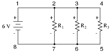
Being a parallel circuit, the voltage across every resistor is the same as the supply voltage: 6 volts. Tallying up voltages around loop 2-3-4-5-6-7-2, we get:

Note how I label the final (sum) voltage as E2-2. Since we began our loop-stepping sequence at point 2 and ended at point 2, the algebraic sum of those voltages will be the same as the voltage measured between the same point (E2-2), which of course must be zero.

The fact that this circuit is parallel instead of series has nothing to do with the validity of Kirchhoff's Voltage Law. For that matter, the circuit could be a "black box" -- its component configuration completely hidden from our view, with only a set of exposed terminals for us to measure voltage between -- and KVL would still hold true:

Try any order of steps from any terminal in the above diagram, stepping around back to the original terminal, and you'll find that the algebraic sum of the voltages always equals zero.

Furthermore, the "loop" we trace for KVL doesn't even have to be a real current path in the closed-circuit sense of the word. All we have to do to comply with KVL is to begin and end at the same point in the circuit, tallying voltage drops and polarities as we go between the next and the last point. Consider this absurd example, tracing "loop" 2-3-6-3-2 in the same parallel resistor circuit:


KVL can be used to determine an unknown voltage in a complex circuit, where all other voltages around a particular "loop" are known. Take the following complex circuit (actually two series circuits joined by a single wire at the bottom) as an example:

To make the problem simpler, I've omitted resistance values and simply given voltage drops across each resistor. The two series circuits share a common wire between them (wire 7-8-9-10), making voltage measurements between the two circuits possible. If we wanted to determine the voltage between points 4 and 3, we could set up a KVL equation with the voltage between those points as the unknown:


Stepping around the loop 3-4-9-8-3, we write the voltage drop figures as a digital voltmeter would register them, measuring with the red test lead on the point ahead and black test lead on the point behind as we progress around the loop. Therefore, the voltage from point 9 to point 4 is a positive (+) 12 volts because the "red lead" is on point 9 and the "black lead" is on point 4. The voltage from point 3 to point 8 is a positive (+) 20 volts because the "red lead" is on point 3 and the "black lead" is on point 8. The voltage from point 8 to point 9 is zero, of course, because those two points are electrically common.

Our final answer for the voltage from point 4 to point 3 is a negative (-) 32 volts, telling us that point 3 is actually positive with respect to point 4, precisely what a digital voltmeter would indicate with the red lead on point 4 and the black lead on point 3:

In other words, the initial placement of our "meter leads" in this KVL problem was "backwards." Had we generated our KVL equation starting with E3-4 instead of E4-3, stepping around the same loop with the opposite meter lead orientation, the final answer would have been E3-4 = +32 volts:

It is important to realize that neither approach is "wrong." In both cases, we arrive at the correct assessment of voltage between the two points, 3 and 4: point 3 is positive with respect to point 4, and the voltage between them is 32 volts.