Friday, January 29, 2010

Semiconductor Materials

Unlike other electron devices, which depend for their functioning on the flow of electric charges through a vacuum or a gas, semiconductor devices make use of the flow of current in a solid. In general, all materials may be classified in three major categories — conductors, semiconductors, and insulators — depending upon their ability to conduct an electric current. As the name indicates, a semiconductor material has poorer conductivity than a conductor, but better conductivity than an insulator.

The materials most often used in semiconductor devices are germanium and silicon. Germanium has higher electrical conductivity ( less resistance to current flow ) than silicon, and is used in most low– and medium–power diodes and transistors. Silicon is more suitable for high–power devices than germanium. One reason is that it can be used at much higher temperatures. A relatively new material which combines the principal desirable features of both germanium and silicon is gallium arsenide. When further experience with this material has been obtained, it is expected to find much wider use in semiconductor devices.

Resistivity

The ability of a material to conduct current ( conductivity ) is directly proportional to the number of free ( loosely held ) electrons in the material. Good conductors, such as silver, copper, and aluminum, have large numbers of free electrons; their resistivities are of the order of a few millionths of an ohm-centimeter. Insulators such as glass, rubber, and mica, which have very few loosely held electrons, have resistivities as high as several million ohm-centimeters.

Semiconductor materials lie in the range between these two extremes, as shown in Fig. 1. Pure germanium has a resistivity of 60 ohm–centimeters. Pure silicon has a considerably higher resistivity, in the order of 60,000 obm-centimeters. As used in semiconductor devices, however, these materials contain carefully controlled amounts of certain impurities which reduce their resistivity to about 2 ohm–centimeters at room temperature ( this resistivity decreases rapidly as the temperature rises ).


Impurities

Carefully prepared semiconductor materials have a crystal structure. In this type of structure, which is called a lattice, the outer or valence electrons of individual atoms are tightly bound to the electrons of adjacent atoms in electron–pair bonds, as shown in Fig. 2. Because such a structure has no loosely held electrons, semiconductor materials are poor conductors under normal conditions. In order to separate the electron pair bonds and provide free electrons for electrical conduction, it would be necessary to apply high temperatures or strong electric fields.


Another way to alter the lattice structure and thereby obtain free electrons, however, is to add small amounts of other elements having a different atomic structure. By the addition of almost infinitesimal amounts of such other elements, called "impurities", the basic electrical properties of pure semiconductor materials can be modified and controlled. The ratio of impurity to the semiconductor material is usually extremely small, in the order of one part in ten million. ( 0.1 ppm )

When the impurity elements are added to the semiconductor material, impurity atoms take the place of semiconductor atoms in the lattice structure. If the impurity atoms added have the same number of valence electrons as the atoms of the original semiconductor material, they fit neatly into the lattice, forming the required number of electron–pair bonds with semiconductor atoms. In this case, the electrical properties of the material are essentially unchanged.

When the impurity atom has one more valence electron than the semiconductor atom, however, this extra electron cannot form an electron pair bond because no adjacent valence electron is available. The excess electron is then held very loosely by the atom, as shown in Fig. 3, and requires only slight excitation to break away. Consequently, the presence of such excess electrons makes the material a better conductor, i.e., its resistance to current flow is reduced.


Impurity elements which are added to germanium and silicon crystals to provide excess electrons include arsenic and antimony. When these elements are introduced, the resulting material is called n–type because the excess free electrons have a negative charge. ( It should be noted, however, that the negative charge of the electrons is balanced by an equivalent positive charge in the center of the impurity atoms. Therefore, the net electrical charge of the semiconductor material is not changed. )

A different effect is produced when an impurity atom having one less valence electron than the semiconductor atom is substituted in the lattice structure. Although all the valence electrons of the impurity atom form electron–pair bonds with electrons of neighboring semiconductor atoms, one of the bonds in the lattice structure cannot be completed because the impurity atom lacks the final valence electron. As a result, a vacancy or "hole" exists in the lattice, as shown in Fig. 4. An electron from an adjacent electron–pair bond may then absorb enough energy to break its bond and move through the lattice to fill the hole. As in the case of excess electrons, the presence of "holes" encourages the flow of electrons in the semiconductor material; consequently, the conductivity is increased and the resistivity is reduced.


The vacancy or hole in the crystal structure is considered to have a positive electrical charge because it represents the absence of an electron. ( Again, however, the net charge of the crystal is unchanged. ) Semiconductor material which contains these "holes" or positive charges is called p–type material. p–type materials are formed by the addition of aluminum, gallium, or indium. Although the difference in the chemical composition of n–type and p–type materials is slight, the differences in the electrical characteristics of the two types are substantial, and are very important in the operation of semiconductor devices.

P–N JUNCTIONS

When n–type and p–type materials are joined together, as shown in Fig. 5, an unusual but very important phenomenon occurs at the interface where the two materials meet ( called "the p-n junction" ). An interaction takes place between the two types of material at the junction as a result of the holes in one material and the excess electrons in the other.


When a p–n junction is formed, some of the free electrons from the n-type material diffuse across the junction and recombine with holes in the lattice structure of the p–type material; similarly, some of the holes in the p–type material diffuse across the junction and recombine with free electrons in the lattice structure of the n–type material. This interaction or diffusion is brought into equilibrium by a small space–charge region ( sometimes called the transition region or depletion layer ). The p–type material thus acquires a slight negative charge and the n–type material acquires a slight positive charge.

Thermal energy causes charge carriers ( electrons and holes ) to diffuse from one side of the p–n junction to the other side; this flow of charge carriers is called diffusion current. As a result of the diffusion process, however, a potential gradient builds up across the space–charge region. This potential gradient can be represented, as shown in Fig. 6, by an imaginary battery connected across the p–n junction. ( The battery symbol is used merely to illustrate internal effects; the potential it represents is not directly measurable. )


The potential gradient causes a flow of charge carriers, referred to as drift current, in the opposite direction to the diffusion current. Under equilibrium conditions, the diffusion current is exactly balanced by the drift current so that the net current across the p–n junction is zero. In other words, when no external current or voltage is applied to the p–n junction, the potential gradient forms an energy barrier that prevents further diffusion of charge carriers across the junction. In effect, electrons from the n–type material that tend to diffuse across the junction are repelled by the slight negative charge induced in the p-type material by the potential gradient, and holes from the p–type material are repelled by the slight positive charge induced in the n–type material. The potential gradient ( or energy barrier, as it is sometimes called ), therefore, prevents total interaction between the two types of materials, and thus preserves the differences in their characteristics.

CURRENT FLOW

When an external battery is connected across a p–n junction, the amount of current flow is determined by the polarity of the applied voltage and its effect on the space–charge region. In. Fig. 7a, the positive terminal of the battery is connected to the n–type material and the negative terminal to the p–type material.


In this arrangement, the free electrons in the n–type material are attracted toward the positive terminal of the battery and away from the junction. At the same time, holes from the p–type material are attracted toward, the negative terminal of the battery and away from the junction. As a result, the space–charge region at the junction becomes effectively wider, and the potential gradient increases until it approaches the potential of the external battery. Current flow is then extremely small because no voltage difference ( electric field ) exists across either the p–type or the n–type region. Under these conditions, the p–n junction is said to be reverse–biased.

In Fig. 7b, the positive terminal of the external battery is connected to the p–type material and the negative terminal to the n–type material.


In this arrangement, electrons in the p–type material near the positive terminal of the battery break their electron–pair bonds and enter the battery, creating new holes. At the same time, electrons from the negative terminal of the battery enter the n–type material and diffuse toward the junction. As a result, the space charge region becomes effectively narrower, and the energy barrier decreases to an insignificant value. Excess electrons from the n–type material can then penetrate the space charge region, flow across the junction, and move by way of the holes in the p–type material toward the positive terminal of the battery. This electron flow continues as long as the external voltage is applied. Under these conditions, the junction is said to be forward–biased.

The generalized voltage–current characteristic for a p–n junction in Fig. 8 shows both the reverse–bias and forward–bias regions.


In the forward–bias region, current rises rapidly as the voltage is increased and is quite high. Current in the reverse–bias region is usually much lower. Excessive voltage ( bias ) in either direction should be avoided in normal applications because excessive currents and the resulting high temperatures may permanently damage the semiconductor device.

N–P–N and P–N–P STRUCTURES

fig.7 shows that a p–n junction biased in the reverse direction is equivalent to a high–resistance element ( low current for a given applied voltage ), while a junction biased in the forward direction is equivalent to a low–resistance element ( high current for a given applied voltage ). Because the power developed by a given current is greater in a high–resistance element than in a low–resistance element ( P=I2R ), power gain can be obtained in a structure containing two such resistance elements if the current flow is not materially reduced. A device containing two p–n junctions biased in opposite directions can operate in this fashion.

Such a two–junction device is shown in Fig. 9.


The thick end layers are made of the same type of material ( n–type in this case ), and are separated by a very thin layer of the opposite type of material ( p–type in the device shown ). By means of the external batteries, the left–hand ( p–n ) junction is biased in the forward direction to provide a low–resistance input circuit, and the right–hand ( p–n ) junction is biased in the reverse direction to provide a high–resistance output circuit. ...

Maximum Power Transfer Theorem

The Maximum Power Transfer Theorem is not so much a means of analysis as it is an aid to system design. Simply stated, the maximum amount of power will be dissipated by a load resistance when that load resistance is equal to the Thevenin/Norton resistance of the network supplying the power. If the load resistance is lower or higher than the Thevenin/Norton resistance of the source network, its dissipated power will be less than maximum.

This is essentially what is aimed for in radio transmitter design , where the antenna or transmission line “impedance” is matched to final power amplifier “impedance” for maximum radio frequency power output. Impedance, the overall opposition to AC and DC current, is very similar to resistance, and must be equal between source and load for the greatest amount of power to be transferred to the load. A load impedance that is too high will result in low power output. A load impedance that is too low will not only result in low power output, but possibly overheating of the amplifier due to the power dissipated in its internal (Thevenin or Norton) impedance.

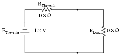
Taking our Thevenin equivalent example circuit, the Maximum Power Transfer Theorem tells us that the load resistance resulting in greatest power dissipation is equal in value to the Thevenin resistance (in this case, 0.8 Ω):

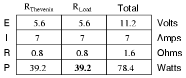
With this value of load resistance, the dissipated power will be 39.2 watts:

If we were to try a lower value for the load resistance (0.5 Ω instead of 0.8 Ω, for example), our power dissipated by the load resistance would decrease:

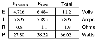
Power dissipation increased for both the Thevenin resistance and the total circuit, but it decreased for the load resistor. Likewise, if we increase the load resistance (1.1 Ω instead of 0.8 Ω, for example), power dissipation will also be less than it was at 0.8 Ω exactly:

If you were designing a circuit for maximum power dissipation at the load resistance, this theorem would be very useful. Having reduced a network down to a Thevenin voltage and resistance (or Norton current and resistance), you simply set the load resistance equal to that Thevenin or Norton equivalent (or vice versa) to ensure maximum power dissipation at the load. Practical applications of this might include radio transmitter final amplifier stage design (seeking to maximize power delivered to the antenna or transmission line), a grid tied inverter loading a solar array, or electric vehicle design (seeking to maximize power delivered to drive motor).

The Maximum Power Transfer Theorem is not: Maximum power transfer does not coincide with maximum efficiency. Application of The Maximum Power Transfer theorem to AC power distribution will not result in maximum or even high efficiency. The goal of high efficiency is more important for AC power distribution, which dictates a relatively low generator impedance compared to load impedance.

Similar to AC power distribution, high fidelity audio amplifiers are designed for a relatively low output impedance and a relatively high speaker load impedance. As a ratio, "output impdance" : "load impedance" is known as damping factor, typically in the range of 100 to 1000.

Maximum power transfer does not coincide with the goal of lowest noise. For example, the low-level radio frequency amplifier between the antenna and a radio receiver is often designed for lowest possible noise. This often requires a mismatch of the amplifier input impedance to the antenna as compared with that dictated by the maximum power transfer theorem.

NODAL ANALYSIS

After simulating circuits for some time, I began to ask myself - how does this SPICE program work? What mathematical tricks does the code execute to simulate complex electrical circuits described by non-linear differential equations? After some searching and digging, some answers were uncovered. At the core of the SPICE engine is a basic technique called Nodal Analysis. It calculates the voltage at any node given all resistances (conductances) and current sources of the circuit. Whether the program is performing DC, AC, or Transient Analysis, SPICE ultimately casts its components (linear, non-linear and energy-storage elements) into a form where the innermost calculation is Nodal Analysis.

WHAT IS NODAL ANALYSIS?

Kirchoff discovered this: the total current entering a node equals the total current leaving a node! And, these currents can be described by an equation of voltages and conductances. If you have more than one node, then you get more than one equation describing the same system (simultaneous equations). The trick now is finding the voltage at each node that satisfies all of the equations simultaneously.

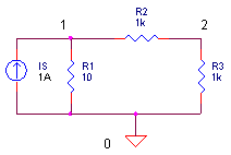
Circuit Example Here’s a simple circuit example.

Another way of stating the KC Law is this: the sum of currents in and out of a node is zero. This makes writing nodal equations a piece of cake. The two equations for the two circuit nodes look like this.

Because our mission is to calculate the node voltages, let’s reorganize the equations in terms of V1 and V2.

So here sit V1 and V2 in the middle of two different equations. The trick is finding the values of V1 and V2 that satisfy both equations. But how?

SOLUTION #1 – WORK THE EQUATIONS

Just roll up your sleeves and solve for V1 and V2. Before we begin we’ll make bookkeeping easy by writing the resistors in terms of total conductance: G11 = 1/R1 + 1/R2, G12 = -1/R2, G21 = -1/R2 and G22 = 1/R2+1/R3. The system equations now look like this.

First, solve the second equation for V1

Then, stick this into the first equation and solve for V2

Okay, it’s a little messy, but we’ve got V2 described by circuit conductances and Is only! After V2 is calculated numerically, stick it back into V1 = – G22 ∙V2 / G21 and there you have it, circuit voltages V1 and V2 that satisfy both system equations.

SOLUTION #2 – THE MATRIX

Solution #1 looks reasonable for simple circuits, but what about medium or large circuits? The bookkeeping of terms spins out of control quickly. What’s needed is a more methodical and efficient solution: Enter the Matrix. Here’s the set of nodal equations written in matrix form.

Or, in terms of total conductances and source currents

Treating each matrix as a variable, you can write

G v = i

In the matrix world, you can solve for a variable (almost) like any other algebraic equation. Solving for v you get

v = G-1 i

Where G-1 is the matrix inverse of G. ( 1 / G does not exist in the matrix world.) This equation is the central mechanism of the SPICE algorithm. Regardless of the analysis – AC, DC, or Transient – all components or their effects are cast into the conductance matrix G and the node voltages are calculated by v = G-1 i , or some equivalent method.

Superposition Theorem

Superposition theorem is one of those strokes of genius that takes a complex subject and simplifies it in a way that makes perfect sense. A theorem like Millman's certainly works well, but it is not quite obvious why it works so well. Superposition, on the other hand, is obvious.

The strategy used in the Superposition Theorem is to eliminate all but one source of power within a network at a time, using series/parallel analysis to determine voltage drops (and/or currents) within the modified network for each power source separately. Then, once voltage drops and/or currents have been determined for each power source working separately, the values are all “superimposed” on top of each other (added algebraically) to find the actual voltage drops/currents with all sources active. Let's look at our example circuit again and apply Superposition Theorem to it:

Since we have two sources of power in this circuit, we will have to calculate two sets of values for voltage drops and/or currents, one for the circuit with only the 28 volt battery in effect. . .

. . . and one for the circuit with only the 7 volt battery in effect:

When re-drawing the circuit for series/parallel analysis with one source, all other voltage sources are replaced by wires (shorts), and all current sources with open circuits (breaks). Since we only have voltage sources (batteries) in our example circuit, we will replace every inactive source during analysis with a wire.

Analyzing the circuit with only the 28 volt battery, we obtain the following values for voltage and current:


Analyzing the circuit with only the 7 volt battery, we obtain another set of values for voltage and current:


When superimposing these values of voltage and current, we have to be very careful to consider polarity (voltage drop) and direction (electron flow), as the values have to be added algebraically.

Applying these superimposed voltage figures to the circuit, the end result looks something like this:

Currents add up algebraically as well, and can either be superimposed as done with the resistor voltage drops, or simply calculated from the final voltage drops and respective resistances (I=E/R). Either way, the answers will be the same. Here I will show the superposition method applied to current:

Once again applying these superimposed figures to our circuit:

Quite simple and elegant, don't you think? It must be noted, though, that the Superposition Theorem works only for circuits that are reducible to series/parallel combinations for each of the power sources at a time (thus, this theorem is useless for analyzing an unbalanced bridge circuit), and it only works where the underlying equations are linear (no mathematical powers or roots). The requisite of linearity means that Superposition Theorem is only applicable for determining voltage and current, not power!!! Power dissipations, being nonlinear functions, do not algebraically add to an accurate total when only one source is considered at a time. The need for linearity also means this Theorem cannot be applied in circuits where the resistance of a component changes with voltage or current. Hence, networks containing components like lamps (incandescent or gas-discharge) or varistors could not be analyzed.

Another prerequisite for Superposition Theorem is that all components must be “bilateral,” meaning that they behave the same with electrons flowing either direction through them. Resistors have no polarity-specific behavior, and so the circuits we've been studying so far all meet this criterion.

The Superposition Theorem finds use in the study of alternating current (AC) circuits, and semiconductor (amplifier) circuits, where sometimes AC is often mixed (superimposed) with DC. Because AC voltage and current equations (Ohm's Law) are linear just like DC, we can use Superposition to analyze the circuit with just the DC power source, then just the AC power source, combining the results to tell what will happen with both AC and DC sources in effect. For now, though, Superposition will suffice as a break from having to do simultaneous equations to analyze a circuit.

Thevenin's Theorem

Thevenin's Theorem states that it is possible to simplify any linear circuit, no matter how complex, to an equivalent circuit with just a single voltage source and series resistance connected to a load. The qualification of “linear” is identical to that found in the Superposition Theorem, where all the underlying equations must be linear (no exponents or roots). If we're dealing with passive components (such as resistors, and later, inductors and capacitors), this is true. However, there are some components (especially certain gas-discharge and semiconductor components) which are nonlinear: that is, their opposition to current changes with voltage and/or current. As such, we would call circuits containing these types of components, nonlinear circuits.

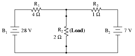
Thevenin's Theorem is especially useful in analyzing power systems and other circuits where one particular resistor in the circuit (called the “load” resistor) is subject to change, and re-calculation of the circuit is necessary with each trial value of load resistance, to determine voltage across it and current through it. Let's take another look at our example circuit:

Let's suppose that we decide to designate R2 as the “load” resistor in this circuit. We already have four methods of analysis at our disposal (Branch Current, Mesh Current, Millman's Theorem, and Superposition Theorem) to use in determining voltage across R2 and current through R2, but each of these methods are time-consuming. Imagine repeating any of these methods over and over again to find what would happen if the load resistance changed (changing load resistance is very common in power systems, as multiple loads get switched on and off as needed. the total resistance of their parallel connections changing depending on how many are connected at a time). This could potentially involve a lot of work!

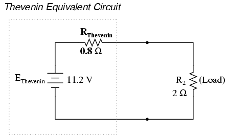
Thevenin's Theorem makes this easy by temporarily removing the load resistance from the original circuit and reducing what's left to an equivalent circuit composed of a single voltage source and series resistance. The load resistance can then be re-connected to this “Thevenin equivalent circuit” and calculations carried out as if the whole network were nothing but a simple series circuit:

. . . after Thevenin conversion . . .

The “Thevenin Equivalent Circuit” is the electrical equivalent of B1, R1, R3, and B2 as seen from the two points where our load resistor (R2) connects.

The Thevenin equivalent circuit, if correctly derived, will behave exactly the same as the original circuit formed by B1, R1, R3, and B2. In other words, the load resistor (R2) voltage and current should be exactly the same for the same value of load resistance in the two circuits. The load resistor R2 cannot “tell the difference” between the original network of B1, R1, R3, and B2, and the Thevenin equivalent circuit of EThevenin, and RThevenin, provided that the values for EThevenin and RThevenin have been calculated correctly.

The advantage in performing the “Thevenin conversion” to the simpler circuit, of course, is that it makes load voltage and load current so much easier to solve than in the original network. Calculating the equivalent Thevenin source voltage and series resistance is actually quite easy. First, the chosen load resistor is removed from the original circuit, replaced with a break (open circuit):

Next, the voltage between the two points where the load resistor used to be attached is determined. Use whatever analysis methods are at your disposal to do this. In this case, the original circuit with the load resistor removed is nothing more than a simple series circuit with opposing batteries, and so we can determine the voltage across the open load terminals by applying the rules of series circuits, Ohm's Law, and Kirchhoff's Voltage Law:


The voltage between the two load connection points can be figured from the one of the battery's voltage and one of the resistor's voltage drops, and comes out to 11.2 volts. This is our “Thevenin voltage” (EThevenin) in the equivalent circuit:

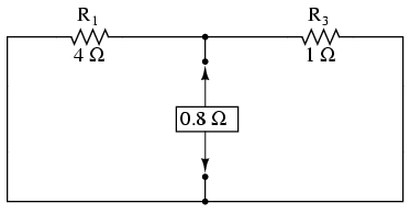
To find the Thevenin series resistance for our equivalent circuit, we need to take the original circuit (with the load resistor still removed), remove the power sources (in the same style as we did with the Superposition Theorem: voltage sources replaced with wires and current sources replaced with breaks), and figure the resistance from one load terminal to the other:

With the removal of the two batteries, the total resistance measured at this location is equal to R1 and R3 in parallel: 0.8 Ω. This is our “Thevenin resistance” (RThevenin) for the equivalent circuit:

With the load resistor (2 Ω) attached between the connection points, we can determine voltage across it and current through it as though the whole network were nothing more than a simple series circuit:

Notice that the voltage and current figures for R2 (8 volts, 4 amps) are identical to those found using other methods of analysis. Also notice that the voltage and current figures for the Thevenin series resistance and the Thevenin source (total) do not apply to any component in the original, complex circuit. Thevenin's Theorem is only useful for determining what happens to a single resistor in a network: the load.

The advantage, of course, is that you can quickly determine what would happen to that single resistor if it were of a value other than 2 Ω without having to go through a lot of analysis again. Just plug in that other value for the load resistor into the Thevenin equivalent circuit and a little bit of series circuit calculation will give you the result.

Norton's Theorem

Norton's Theorem states that it is possible to simplify any linear circuit, no matter how complex, to an equivalent circuit with just a single current source and parallel resistance connected to a load. Just as with Thevenin's Theorem, the qualification of “linear” is identical to that found in the Superposition Theorem: all underlying equations must be linear (no exponents or roots).

Contrasting our original example circuit against the Norton equivalent: it looks something like this:

. . . after Norton conversion . . .

Remember that a current source is a component whose job is to provide a constant amount of current, outputting as much or as little voltage necessary to maintain that constant current.

As with Thevenin's Theorem, everything in the original circuit except the load resistance has been reduced to an equivalent circuit that is simpler to analyze. Also similar to Thevenin's Theorem are the steps used in Norton's Theorem to calculate the Norton source current (INorton) and Norton resistance (RNorton).

As before, the first step is to identify the load resistance and remove it from the original circuit:

Then, to find the Norton current (for the current source in the Norton equivalent circuit), place a direct wire (short) connection between the load points and determine the resultant current. Note that this step is exactly opposite the respective step in Thevenin's Theorem, where we replaced the load resistor with a break (open circuit):

With zero voltage dropped between the load resistor connection points, the current through R1 is strictly a function of B1's voltage and R1's resistance: 7 amps (I=E/R). Likewise, the current through R3 is now strictly a function of B2's voltage and R3's resistance: 7 amps (I=E/R). The total current through the short between the load connection points is the sum of these two currents: 7 amps + 7 amps = 14 amps. This figure of 14 amps becomes the Norton source current (INorton) in our equivalent circuit:

Remember, the arrow notation for a current source points in the direction opposite that of electron flow. Again, apologies for the confusion. For better or for worse, this is standard electronic symbol notation. Blame Mr. Franklin again!

To calculate the Norton resistance (RNorton), we do the exact same thing as we did for calculating Thevenin resistance (RThevenin): take the original circuit (with the load resistor still removed), remove the power sources (in the same style as we did with the Superposition Theorem: voltage sources replaced with wires and current sources replaced with breaks), and figure total resistance from one load connection point to the other:

Now our Norton equivalent circuit looks like this:

If we re-connect our original load resistance of 2 Ω, we can analyze the Norton circuit as a simple parallel arrangement:

As with the Thevenin equivalent circuit, the only useful information from this analysis is the voltage and current values for R2; the rest of the information is irrelevant to the original circuit. However, the same advantages seen with Thevenin's Theorem apply to Norton's as well: if we wish to analyze load resistor voltage and current over several different values of load resistance, we can use the Norton equivalent circuit again and again, applying nothing more complex than simple parallel circuit analysis to determine what's happening with each trial load.